
08
21
2018
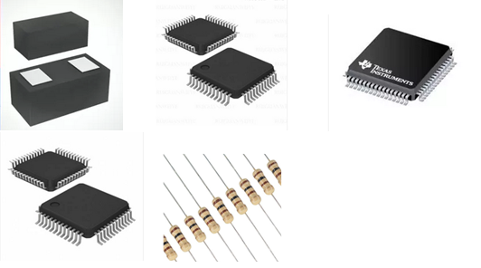
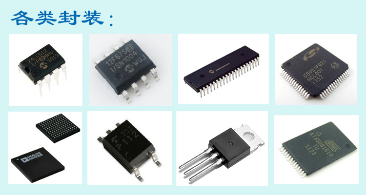
MSP430F425AIPMR/MSP430F449IPZR
来源:[誉诚(深圳)实业科技有限公司]
联系人:朱女士
手机:13560767759
电话:0755-29309513
传真:0755-29309513
QQ:1831176842
Email:siruitegs@163.com
地址:广东省深圳市深圳市深圳市福田区赛格电子科技大厦
品牌:TI
价格:6.30
元/只
供应地:广东省深圳市
产品型号:MSP430F425AIPMR
peripherals
Peripherals are connected to the CPU through data, address, and control buses and can be handled using all
instructions. For complete module deSCRJPTions, see the MSP430x4xx Family User’s Guide, literature number
SLAU056.
oscillator and system clock
The clock system in the MSP430F42xA family of devices is supported by the FLL+ module, which includes
support for a 32768-Hz watch crystal oscillator, an internal digitally-controlled oscillator (DCO), and a
high-frequency crystal oscillator. The FLL+ clock module is designed to meet the requirements of both low
system cost and low power consumption. The FLL+ features digital frequency locked loop (FLL) hardware that,
in conjunction with a digital modulator, stabilizes the DCO frequency to a programmable multiple of the watch
crystal frequency. The internal DCO provides a fast turn-on clock source and stabilizes in less than 6 μs. The
FLL+ module provides the following clock signals:
D
Auxiliary clock (ACLK), sourced from a 32768-Hz watch crystal or a high-frequency crystal.
D
Main clock (MCLK), the system clock used by the CPU.
D
Sub-Main clock (SMCLK), the subsystem clock used by the peripheral modules.
D
ACLK/n, the buffered output of ACLK, ACLK/2, ACLK/4, or ACLK/8.
brownout, supply voltage supervisor (SVS)
The brownout circuit is implemented to provide the proper internal reset signal to the device during power on
and power off. The SVS circuitry detects if the supply voltage drops below a user-selectable level and supports
both supply-voltage supervision (the device is automatically reset) and supply-voltage monitoring (SVM) (the
device is not automatically reset).
The CPU begins code execution after the brownout circuit releases the device reset. However, VCC may not
have ramped to VCC(min) at that time. The user must ensure the default FLL+ settings are not changed until VCC
reaches VCC(min). If desired, the SVS circuit can be used to determine when VCC reaches VCC(min
